Project Description
Main Project Image
The project owner hasn't added main project image yet.
Project description
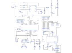
This development board contain only the switching regulator (to generate +5V DC from the input power source) and RS232 serial port interface. The switching regulator of this development board may support input voltage of +8V to +25V DC. RS232 Serial interface of this development board is based on Maxim's MAX232 driver/receiver IC.
This given design has 6 two-way jumpers to select crystal oscillator, MCLR and RS232 Tx/Rx terminals.
While at the prototyping stages we test this board successfully with PIC16F887, PIC16F877/A, PIC18F452, PIC18F4550 and PIC18F4620 MCUs. A dimension of this PIC Development Board is 110×85mm.
Schematic, PCB design and some of the related documents of this project are licensed under the Creative Commons Attribution-ShareAlike 3.0 Unported License.
Gallery
The project owner hasn't added any images yet.
Design Files
Embed Code
Component (28)
Qty
Description
resistor:R-US_:0204/7
R5, R4, R6
3
resistor:R-US_:0204/7
rcl:CPOL-US:E2.5-7
C8, C7, C6, C9
4
rcl:CPOL-US:E2.5-7
supply1:VCC:
P+4, P+3, P+2, P+6, P+5, P+1
6
supply1:VCC:
jumper:JP2E:
JP4, JP1, JP5, JP3, JP2
5
jumper:JP2E:
